



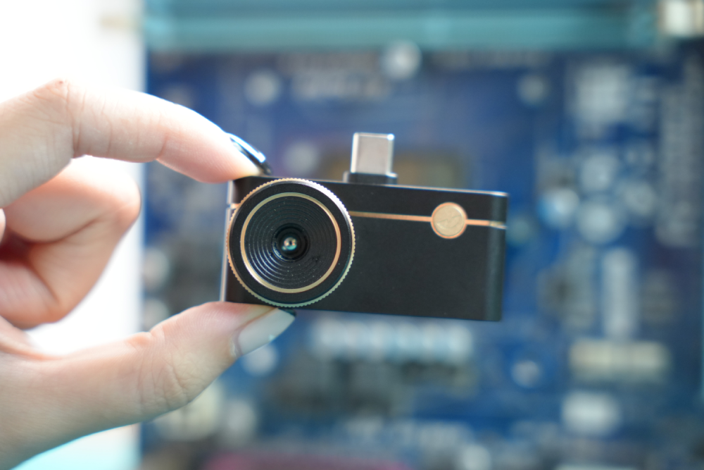
Thermal cameras for PCB repair can help technicians identify PCB problems that are difficult to detect through visual inspection alone.
Electronics repair technician Mike Harris was troubleshooting an industrial motor-control system that had begun experiencing intermittent shutdowns. To find the source of the problem, he used the Thermal Master P3 to scan the circuit boards and compare their thermal patterns, looking for unusual temperature changes that could help pinpoint the fault.
How Do PCB Components Overheat?
Mike starts by scanning the power section, where MOSFETs, capacitors, and other components are packed closely together. To the naked eye, the boards look almost identical, and there may be no visible signs of damage. A component can still be running hotter than expected even when its surface looks completely normal.

P3’s NETD is below 35 mK, meaning it can capture very subtle temperature differences and make small changes in thermal patterns easier to see. This is where a thermal camera for PCB repair can add another layer of information to conventional inspection. Instead of relying only on visible damage or electrical readings, Mike can see how heat is distributed across the board and identify areas that deserve closer attention.

Seeing What the Naked Eye Cannot
Once Mike had identified the hotspot, he moved closer to the MOSFET and adjusted the P3’s manual focus to examine the component and nearby solder joints. The X³IR algorithm enhanced the thermal image up to 512 × 384, making it easier to distinguish the hotspot from the surrounding board area.
Mike then used the P3’s temperature measurement tools to compare the suspect MOSFET with the same component on the known-good board. The difference was significant: the suspect component reached around 120°C, while the corresponding component on the good board remained below 75°C.

This gave him a specific place to continue testing. The thermal image showed where the abnormal heat was developing, but it did not tell him what was causing it. Mike used a multimeter to check the MOSFET and the surrounding power circuit, eventually confirming that the MOSFET was faulty.
From Hot Spot to Final Repair
Mike replaced the faulty MOSFET and ran the system through the same load cycle. He then scanned the board again with the P3. The previous hotspot was gone, and the temperature distribution around the power section was much closer to that of the known-good board.

He also checked other boards from the same batch, focusing on the area where the original problem had appeared. This allowed him to look for similar thermal patterns before another board developed the same shutdown issue.
The P3 can also be used beyond the initial inspection. Thermal images can be transferred to a PC for further analysis, allowing technicians to review temperature readings, compare images, and keep inspection results for later reference.

In this case, the process was straightforward: the P3 revealed an abnormal thermal pattern, helped narrow the problem down to one component, and confirmed that the hotspot disappeared after the repair. For technicians looking for a thermal camera for PCB repair, that makes thermal imaging a practical addition to the electrical tools already used on the bench.
Read More
Thermal Cameras for PCB Inspection: 3 Ways to Improve Troubleshooting
Best Thermal Camera 2025 for PCB Engineers? Meet the Thermal Master P3

Hinterlasse einen Kommentar
Alle Kommentare werden vor der Veröffentlichung geprüft.
Diese Website ist durch hCaptcha geschützt und es gelten die allgemeinen Geschäftsbedingungen und Datenschutzbestimmungen von hCaptcha.