


Many DIY electronics enthusiasts and professional technicians wonder if a thermal camera is sensitive enough to detect minute current leaks on a PCB (Printed Circuit Board). The short answer is yes. The capability depends on specific features like macro focus and high thermal sensitivity.
This article explains the key requirements for PCB leak detection and how to achieve it with the right phone thermal camera.
Do phone Thermal Cameras Work for Electronics Diagnostics?
The world of thermal imaging has dramatically changed. While bulky, expensive handheld units were once the only option for professional work, modern phone attachments have entered the arena. But can they truly handle precision tasks like PCB diagnostics?
The core principle certainly applies: any electrical fault that generates heat can be revealed through thermal imaging. However, not every phone thermal camera is created equal for this task. Standard models might be great for finding house drafts, but they often lack the fine detail needed for electronics.
The gap lies in specialization. Advanced models designed for engineers and technicians now bridge this gap. They transform your phone into a diagnostic tool. This isn't just about spotting a hot component; it's about preventive maintenance and pinpoint accuracy for electrical inspection.
What Features Does a Phone Thermal Camera Need for PCB Inspection?
Whether a phone thermal camera is suitable for PCB leak detection depends on several key technical features, which are outlined below.
Three features are absolutely critical: the ability to see up close, thermal Sensitivity and resolution.
Macro Focus
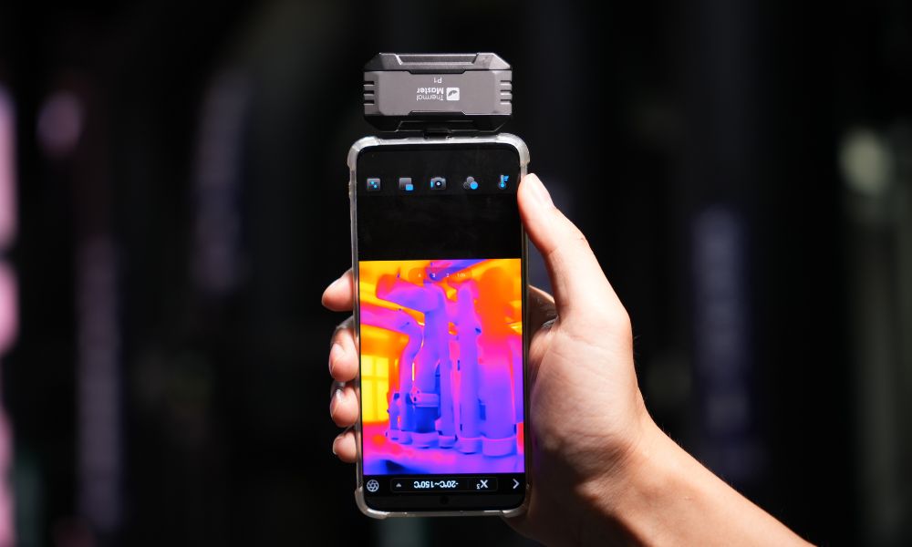
This is the most common limitation of standard thermal cameras. Their lenses are designed for surveying rooms or large objects at a distance, not for close-up electronic work. When brought within centimeters of a PCB, the image quickly becomes blurred, making diagnosis impossible. An 8 mm manual-focus macro lens allows the camera to work at true close range, clearly isolating the heat signature of individual resistors, capacitors, or ICs only millimeters apart.
Thermal Sensitivity
A 1 mA current leak generates extremely little heat, often only a tiny temperature rise that is easy to miss. High thermal sensitivity, commonly measured as NETD, determines whether these faint signals can be detected at all. If sensitivity is insufficient, abnormal heat patterns never appear clearly on screen, no matter how sharp the image looks. For PCB diagnostics, the ability to detect very small temperature differences is essential for identifying hidden faults early and preventing larger failures.
Resolution
Sensitivity is not enough if the sensor does not have enough pixels. On densely populated PCBs, a low-resolution sensor such as 80×60 cannot show where heat is actually building up, and thermal information is blurred across multiple components. A native resolution of 256×192 or higher provides the pixel density needed to localize heat on a specific pin, solder joint, or chip body.

How to Detect PCB Leaks with a Phone Thermal Camera?
Once these conditions are met, phone thermal imaging can be applied to practical PCB leak detection. Here’s a practical guide to using your phone's thermal camera for PCB diagnostics.
Power & Environment Prep
Ensure the PCB is powered, ideally under the conditions where the fault occurs (e.g., booting up, under load). Work in a stable indoor environment away from direct sunlight or strong drafts, which can create misleading thermal patterns.
Camera Configuration
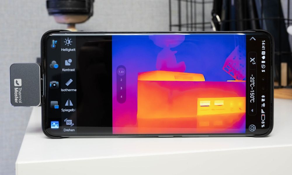
This is key. In your thermal imaging app, set the material emissivity correctly. For a typical PCB laminate, start with a setting around 0.95. Manually adjust the macro lens for the sharpest focus on the components you're inspecting. Enable any high-resolution or enhancement modes (like X³ mode) for maximum detail.
Systematic Scanning
Don't just point and shoot. Slowly and methodically scan the board. Pay special attention to power rails, voltage regulators, DC-DC converters, and connectors. Compare the thermal signature of identical components (e.g., all the RAM chips). One that is noticeably warmer likely has an issue.
Analyze Thermal Anomalies
Look for unexpected "hot spots" which indicate excessive current draw or resistance. Also, watch for unusual "cold spots" which might signal a component that isn't functioning at all. The precise image from the best thermal camera helps you distinguish between a warm IC and a dangerously hot one.
Document for Action
Use your camera's app to capture clear still images and record short videos of the fault. Many apps, including those for professional tools, allow you to generate quick reports or annotate images. This documentation is invaluable for proving the issue, planning the repair, and verifying the fix afterwards.
How to Choose Your Thermal Camera for PCB Diagnostic?
Once you understand how thermal imaging is used to locate PCB leaks, the next step is choosing a thermal camera that can actually deliver these results. Selecting the right tool requires a prioritized checklist:
- Macro Focus First: This is your gateway to clear PCB thermal imaging. Ensure the device specifies a close minimum focus distance.
- Evaluate Sensitivity Resolution: Look for a low NETD value (higher sensitivity) and a high native sensor resolution. Software enhancements are a valuable bonus.
- Consider the Temperature Range: Your thermal camera should cover from near-ambient temperatures (to see subtle leaks) up to high temperatures for overloaded components.
- Battery Life Matters: PCB diagnostics can be time-consuming. Look for a device with long battery life or efficient phone-powered operation.
- Software for Workflow: Robust app features like report generation, adjustable emissivity, and various color palettes are not gimmicks. They optimize your diagnostic workflow. This is why such tools are valued by HVAC and electrical contractors from New York to California.

What Are the Best Phone Thermal Cameras for PCB Work?
For professionals and serious hobbyists, the choice becomes clear when evaluating the necessary features. TheThermal Master P3 is engineered for this challenge. Its defining combination of the 8mm macro lens, X³-enhanced clarity, and a wide measurement range (-4°F to 1112°F) makes it uniquely capable for electronics work.
Consider the case of an Austin, Texas phone repair shop. They faced a consumer device with rapid battery drain. Using the P3's macro focus and high sensitivity, they isolated the fault to a specific faulty Power Management IC (PMIC).
While other phone thermal cameras exist, they often compromise on the macro capability, resolution, or temperature range. These compromises directly limit their effectiveness for the precise, close-up world of PCB inspection.
Conclusion
A modern phone thermal imaging device, specifically one equipped with a macro lens and high thermal sensitivity, transforms from a simple gadget into an excellent diagnostic tool. It empowers you to find not just blatant shorts, but the subtle, energy-wasting leaks that lead to premature failure.
By choosing a device designed for engineering precision, you bring laboratory-grade diagnostic insight directly into your workshop, saving significant time and preventing costly downstream failures.
FAQs
Can I use a regular thermal camera for PCB inspection?
Typically, no. Most standard handheld thermal cameras are designed for building inspections and have a fixed-focus lens that cannot clearly image objects closer than a foot or two away. This renders them nearly useless for seeing tiny PCB components. A dedicated phone attachment with a true macro lens is far more effective and affordable for this specific task.
What is a safe temperature range for PCB components?
Consistent operation near or above a component's rated maximum temperature, as revealed by thermal imaging, is a clear indicator of stress or impending failure.
Can thermal cameras detect short circuits?
Absolutely, and often very clearly. A short circuit typically creates a very localized, intense hot spot due to excessive, unrestricted current flow. This generates a significant amount of heat in a very small area, making it a glaringly obvious target for even a modestly sensitive thermal imaging camera. It is one of the most straightforward faults to identify with this technology.
Related Reading:
Leave a comment
All comments are moderated before being published.
This site is protected by hCaptcha and the hCaptcha Privacy Policy and Terms of Service apply.