


In today's technologically driven world, Printed Circuit Boards (PCBs) are the backbone of numerous electronic devices. However, ensuring their functionality and reliability is paramount. This is where thermal imaging technology comes into play, offering invaluable insights into PCB inspection and repair processes.
Importance of PCB Inspection
PCB defects can lead to malfunctioning electronic devices, resulting in costly repairs and potential damage to brand reputation. Detecting and addressing these defects early can save both time and resources.
Understanding Thermal Imaging for PCB Inspection
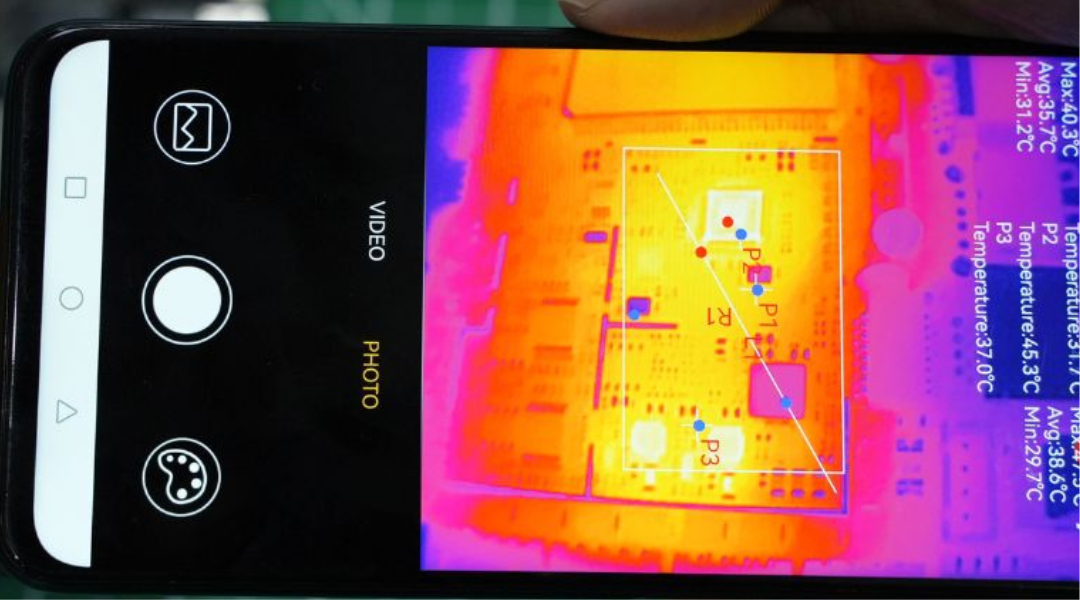
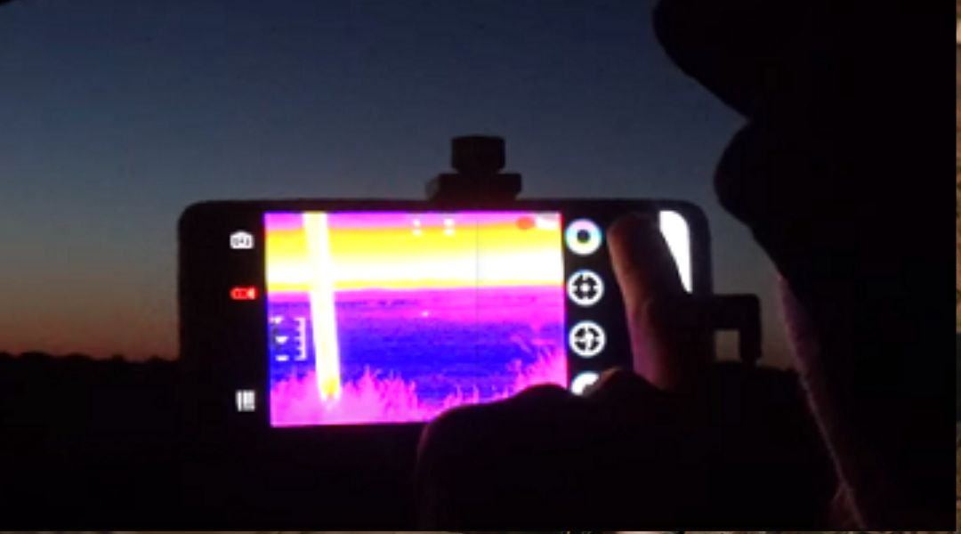
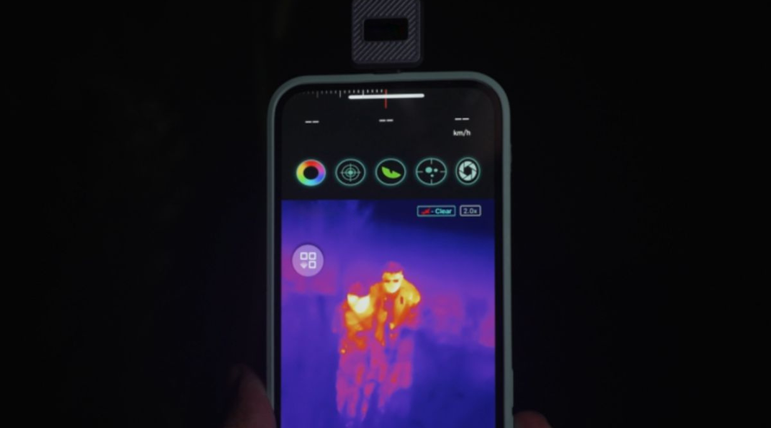
Thermal imaging utilizes infrared radiation to capture temperature variations on a surface. This technology is highly effective for PCB inspection due to its ability to detect heat signatures associated with faulty components or connections.
Killer Tips for Effective PCB Inspection with Thermal Imaging Camera
Proper setup and calibration:
Ensure your thermal imaging camera is calibrated correctly to provide accurate temperature readings. Additionally, optimize camera settings for the specific PCB inspection environment.
Understanding thermal signatures:
Familiarize yourself with the typical thermal signatures of various PCB components, such as resistors, capacitors, and integrated circuits. This knowledge will aid in identifying anomalies during inspection.
Identifying common defects:
Utilize thermal imaging to detect common PCB defects such as overheating components, soldering defects, and short circuits. Pay attention to temperature variations that deviate from the norm.
Real-time monitoring:
Employ real-time thermal imaging monitoring during PCB operation to identify potential issues before they escalate. This proactive approach can prevent costly downtime and repairs.
Integration with other methods:
Combine thermal imaging with other inspection methods, such as visual inspection and electrical testing, for a comprehensive analysis of PCB health.
Best Practices for PCB Repair Guided by Thermal Imaging
Locating faulty components:
Use thermal imaging to pinpoint overheating components or areas on the PCB. This precise localization streamlines the repair process and minimizes downtime.
Precision soldering:
When repairing PCBs, rely on thermal imaging to guide precision soldering techniques. Monitor temperature changes in real-time to ensure proper soldering and prevent damage to surrounding components.
Validation through thermal imaging:
After repair, validate the effectiveness of the repair using thermal imaging. Verify that temperature variations associated with the fault have been resolved, ensuring the PCB's reliability.
Thermal imaging technology offers unparalleled capabilities for PCB inspection and repair, enabling early detection of defects and ensuring the reliability of electronic devices. By following the killer tips outlined in this article, manufacturers can streamline their inspection and repair processes, ultimately improving product quality and customer satisfaction.
Leave a comment
All comments are moderated before being published.
This site is protected by hCaptcha and the hCaptcha Privacy Policy and Terms of Service apply.