In the intricate world of electronics, the decision to fix or replace a faulty component on a Printed Circuit Board (PCB) is a critical one. The advent of thermal imaging technology has revolutionized this process, providing technicians with a powerful tool to diagnose and repair PCBs with precision. This article explores how thermal imaging guides the repair of PCB components, offering a detailed look at its capabilities and benefits.
Understanding PCB and Component Failures
PCBs are the backbone of modern electronic devices, with components soldered onto them to create functional circuits. Failures can occur due to a variety of reasons, including mechanical stress, thermal cycling, and electrical overstress. Identifying the root cause of a failure is the first step in deciding whether to repair or replace the component.
The Role of Thermal Imaging in PCB Repairs
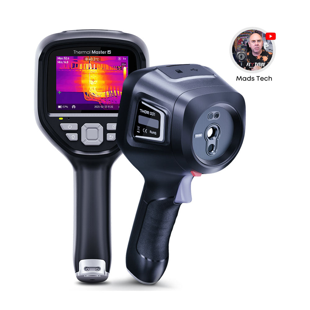
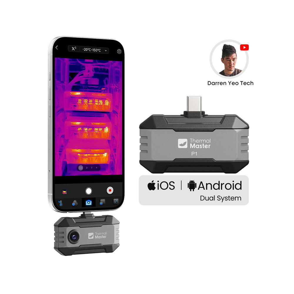
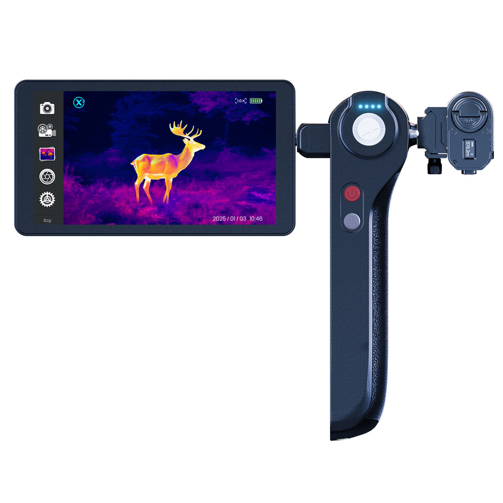
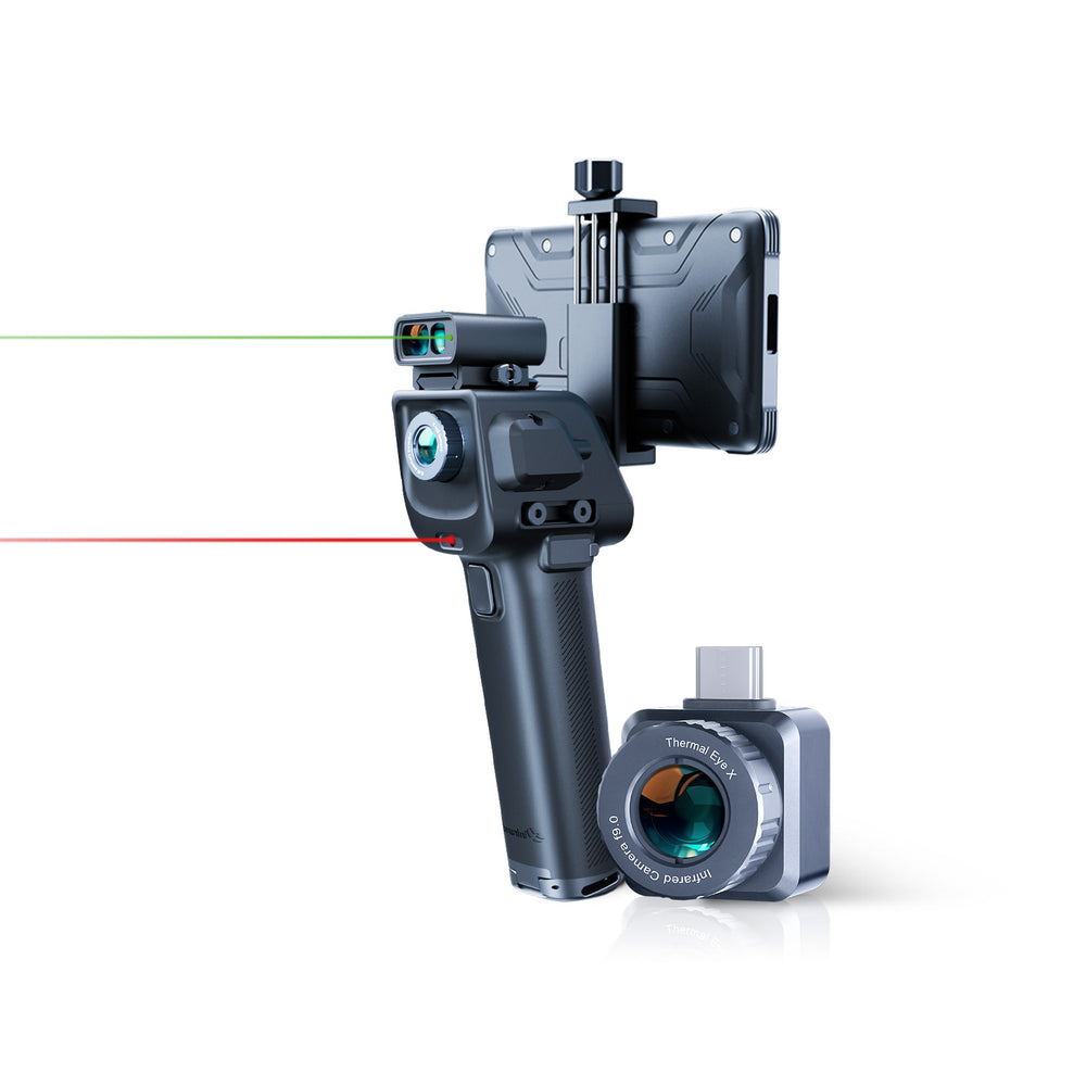
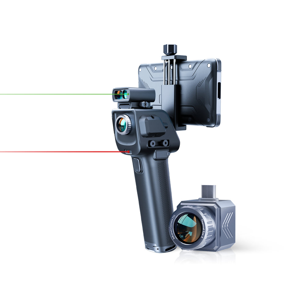
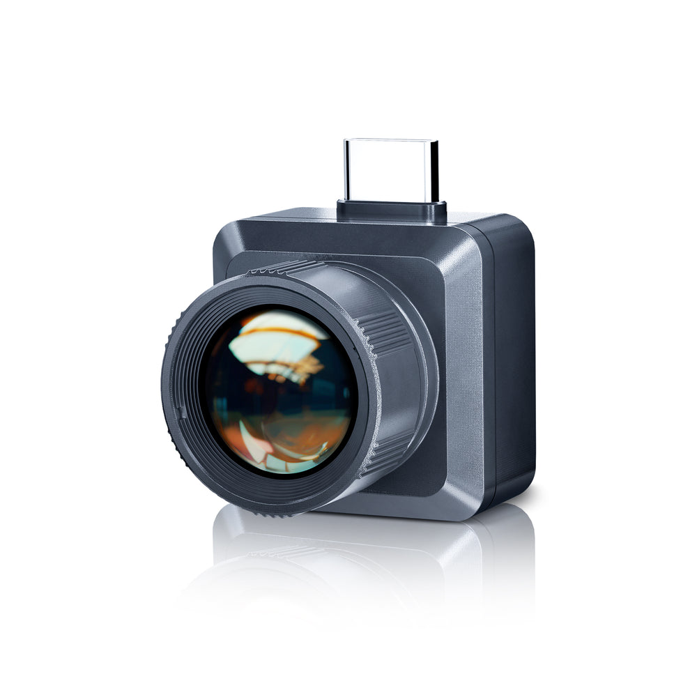
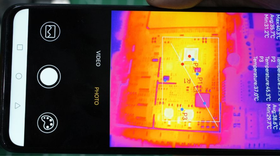
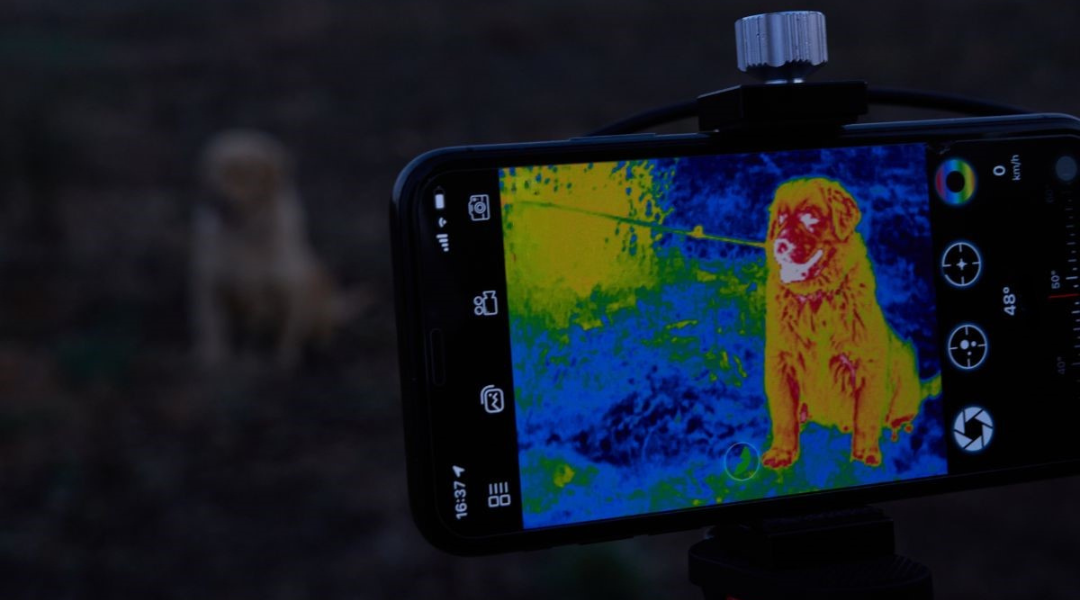
Thermal imaging, also known as thermography, uses infrared cameras to capture heat patterns emitted by objects. In PCB repairs, it allows technicians to visualize temperature variations that indicate potential issues. This non-contact, non-destructive method is invaluable for pinpointing the exact location of a fault.
Identifying Faulty Components
Using thermal imaging, technicians can detect hotspots that suggest component failure. Overheating components can be identified by their abnormal temperature profiles, which stand out against the cooler surrounding areas. This early detection can prevent further damage and system failure.
Assessing the Need for Repair vs. Replacement
The decision to repair or replace a component involves considering several factors, including the cost of repair versus the cost of a new component, the availability of replacement parts, and the potential risks associated with repair. Thermal imaging provides the necessary insights to make an informed decision, balancing economic and practical considerations.
The Repair Process Using Thermal Imaging
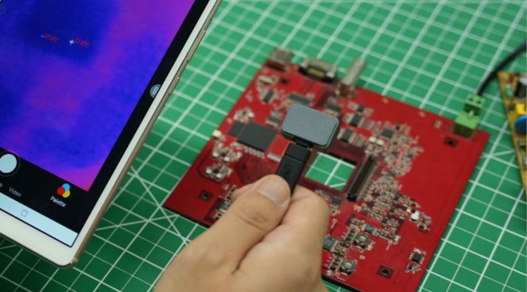
The repair process begins with a thorough thermal scan of the PCB to identify the faulty component. Once identified, the technician can desolder the component, repair or replace it, and then use thermal imaging again to confirm that the repair has resolved the issue. This iterative process ensures the repair is successful and the component is functioning within normal parameters.
Challenges and Limitations
While thermal imaging offers significant advantages, it also has its limitations. Factors such as the size of the component, the materials used, and the complexity of the PCB can affect the accuracy of thermal imaging. Additionally, some components may require specialized knowledge or tools for repair.
The Future of Thermal Imaging in Electronics Repair
As technology advances, thermal imaging is expected to become even more sophisticated, with higher resolution cameras and improved software for analysis. This evolution will likely lead to greater accuracy in diagnosing PCB issues and a more streamlined repair process.
Best Practices for PCB Repairs Using Thermal Imaging
When using thermal imaging for PCB repairs, it's important to follow best practices, including conducting a thorough initial scan, documenting findings, using appropriate repair techniques, and verifying the repair with a follow-up scan. Safety precautions, such as wearing protective gear and working in a well-ventilated area, should also be observed.
Thermal imaging has become an indispensable tool in the field of electronics repair, guiding technicians through the process of identifying, assessing, and repairing PCB components. By providing a clear visual representation of temperature anomalies, it aids in making informed decisions about whether to fix or replace a component. As the technology continues to evolve, its role in PCB repair is set to become even more significant.





Leave a comment
All comments are moderated before being published.
This site is protected by hCaptcha and the hCaptcha Privacy Policy and Terms of Service apply.